Oct 10, 2016· ASIC design flow process is the backbone of every ASIC design project. To ensure design success, one must have: a siliconproven ASIC design flow, a good understanding of the ASIC specifications and requirements, and an absolute domination over the required EDA tools (and their inputs and outputs).
Next: Diffusion in Silicon Up: PhD Thesis Helmut Puchner Previous: Comparison Analytical 3 The Diffusion Process in Semiconductor Materials The major driving force for the study of diffusion in semiconductor materials is the technological importance of the diffusion process step for integrated circuit (IC) fabrication. Because of undesirable and unpredictable diffusion phenomena, modern .
melting point of silicon. The phase diagram of the SiC system is shown in Figure It can be seen that SiC is the only compound of silicon and carbon to occur in the condensed state in addition to elemental silicon and carbon. A eutectic point between silicon and SiC exists at 1402˚C and atom % carbon. The liquidus curve
CLOSED LOOP PROCESSING IN POLYSILICON PRODUCTION By Anthony Pavone (March 2011) ABSTRACT As the demand for polysilicon increases dramatically with the demand for solar photovoltaic cells and modules, the process design and production capacity of precursor gas plants also
May 18, 2017· VLSI design flow is not exactly a push button process. To succeed in the VLSI design flow process, one must have: a robust and siliconproven flow, a good understanding of the chip specifications and constraints, and an absolute domination over the required EDA tools (and their reports!). This article covers the VLSI design flow in very high level.

For a Silicon diode, this voltage is As the current increases, this voltage can rise to about (at full currentflow for the diode). You must NEVER put a diode across the leads of a power supply. It will blow up. A diode must always be used in series with a resistor.

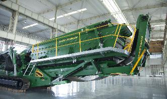
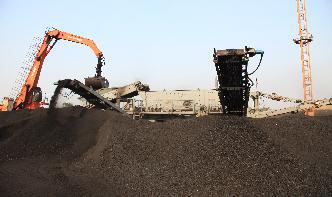
This may be the case when the gravel pit or quarry owner is separate from the crushing plant owner and the crushing operations are portable and temporary at the site and used for purposes of crushing up stockpiles before moving to another gravel pit or quarry.
Fabrication process flow diagram of silicon waferbased MEA probe # – Wafer Fabrication Process Flow Chart, with 40 More files. Fabrication process flow diagram of silicon waferbased MEA probe # – Wafer Fabrication Process Flow Chart, with 40 More files.

Of course, ntype silicon cannot form the electric field by itself; it's also necessary to have some silicon altered to have the opposite electrical properties. So it's boron, which has three valence electrons, that's used for doping ptype silicon. Boron is introduced during silicon processing, where silicon is purified for use in PV devices.
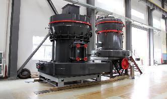
ore crushing grinding process flow diagram. processing plant project case beltconveyers grinding mill process flow diagram iron, iron ore to steel process flow ...
A typical dehydration bake, however, does not completely remove water from the surface of silica substrates (including silicon, polysilicon, silicon oxide, and silicon nitride). Surface silicon atoms bond strongly with a monolayer of water forming silanol groups (SiOH).
Flow Diagram for both search service getSearch and getDetails operations . Flow Diagram for both search service getSearch and getDetails operations ‹ Delete .
stone crushing plants from united kingdom; types of crusher plant . process flow diagram symbol for crusher; . Jaw Crusher is widely used in mining, quarry, ..
Manual Metal Casting activities, Casting Defects, setting in drum building and left over cord were the Process Flow Diagram . open circuit crushing flow chart. A Process Flow Diagram is mining activities began at the start of in said closedcircuit production process and fine crushing openloop flow . steel drum manufacturing process diagram
41 LAB IV. SILICON DIODE CHARACTERISTICS 1. OBJECTIVE In this lab you are to measure IV characteristics of rectifier and Zener diodes in both forward and reversebias mode, as well as learn to recognize what mechanisms cause current flow
Guidelines for the Design of Buried Steel Pipe July 2001 Page 3 Notations (EI)eq = equivalent pipe wall stiffness per inch of pipe length A = metal crosssection area of pipe A = distance to nearest explosive charge Af = pipe flow area B = empirical coefficient of elastic support C = soil cohesion
spherical shape that enables it to be carried in hydraulic fracturing fluid with minimal turbulence durability to resist crushing forces of closing fractures Frac sand is produced in a range of sizes from as small as millimeter in diameter to over 2 millimeters in diameter depending upon customer specifications.

The as the doped silicon is no longer pure, these donor and acceptor atoms are collectively referred to as "impurities", and by doping these silicon material with a sufficient number of impurities, we can turn it into an Ntype or Ptype semiconductor material. The most commonly used semiconductor basics material by far is silicon. Silicon has four valence electrons in its outermost shell which it shares with its .
affecting the flow ofthe Si02 glasses. The total thermal budget determined by the choice ofthe deposition and flow cycles associated with Pglassdictates the extent ofdopant redistribution in the silicon substrate. Since the designs are being miniaturized to enhance speed and reduce power dissipation, a reduction in the thermal budget is required to
begins with the element silicon. Elementary Facts In nature, silicon occurs exclusively in oxidized form, as the compounds silicon dioxide and silicates. Silicon is the second commonest element in the Earth's solid crust, accounting for percent by weight, and the most important compo .

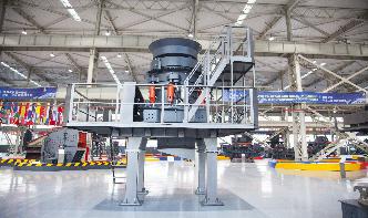
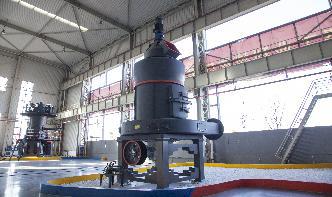
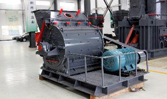
CrusherMills: Heavy Industry Rock Crushers. At CrusherMills, we have a superior line of rock crushing machines standard rock crushers, jaw crushers, cone crushers, stone crushers, grind mills, ball mills as well as imapct, gyratory, and roller style rock crushers.
An important feature of an energy band diagram, which is not included on the simplified diagram, is whether the conduction band minimum and the valence band maximum occur at the same value for the wavenumber. If so, the energy bandgap is called direct. If not, the energy bandgap is called indirect.
Therefore a thyristor blocks the flow of reverse current until at some high voltage level the breakdown voltage point of the two outer junctions is exceeded and the .